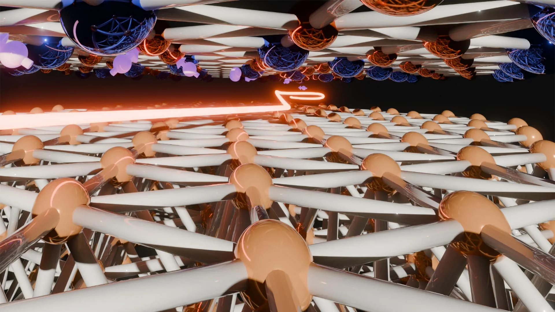
Scientists at the University of Osaka directly observed a heavy fermion state forming where a single atomic layer of ytterbium and copper meets a copper crystal. In this state, electrons behave as though they carry much greater mass than normal. The researchers created the atomic layer on the copper surface and used synchrotron light to study electron interactions at the boundary.
The experiments revealed two separate heavy fermion states with different characteristics. One existed primarily within the two-dimensional atomic layer, while the other extended into the three-dimensional copper crystal below. The second state provided the first direct evidence of heavy fermion behavior generated by interactions across such an interface.
The effect arose from hybridization of localized ytterbium 4f electrons in the atomic layer with mobile conduction electrons in the copper substrate. This interaction showed how combining materials with different electronic properties can produce quantum behavior that neither material exhibits alone.
"This achievement was made possible by our continued efforts to create high-quality materials and measure their electronic states as precisely as possible," says senior author Professor Shin-ichi Kimura. "Our next goal is to engineer and control such heavy-electron states, opening the way to previously unexplored quantum states, including unconventional superconductivity."
The findings suggest that boundaries between materials could become tools for creating exotic quantum states. Future work may adjust interface structures, control electronic orbitals, and manipulate moire patterns to produce and fine-tune quantum phenomena in materials with extremely small dimensions.