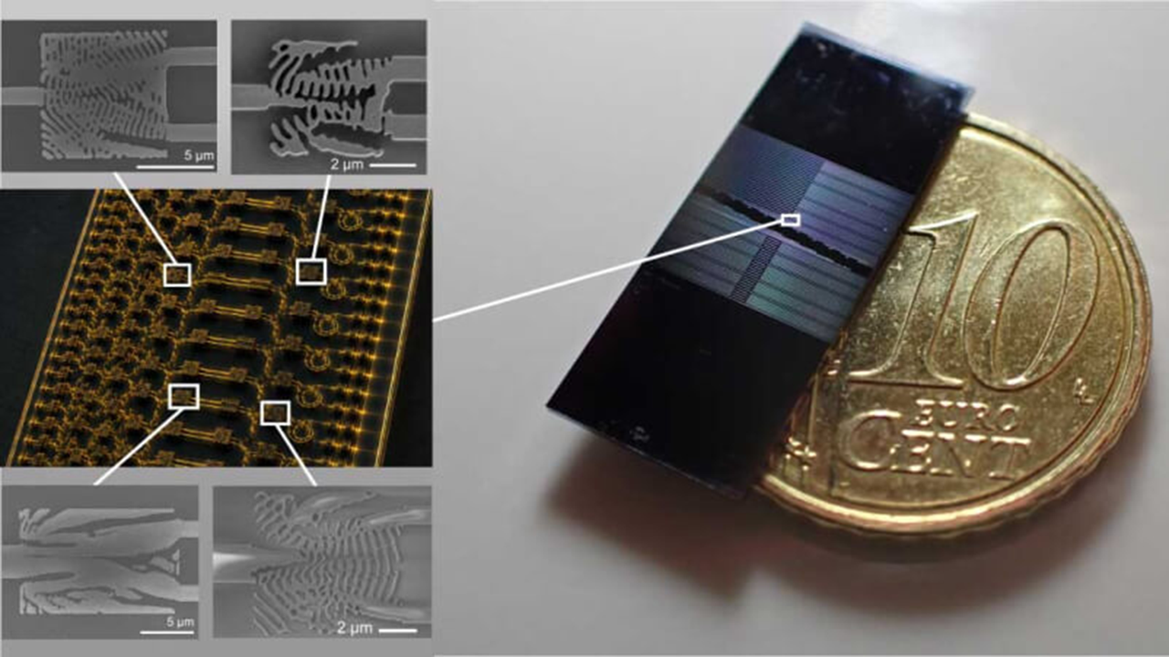
Researchers have created three new chip components using artificial intelligence that measure just a few micrometers long, pushing far beyond the scale human engineers traditionally design at.
The AI-designed structures achieve dimensions approximately 500 times smaller than what conventional engineering approaches produce. This breakthrough demonstrates how machine learning systems can explore design spaces inaccessible to human intuition and manual calculation.
The components represent a fundamental shift in how semiconductor engineers approach miniaturization. Traditional chip design relies on human expertise, physics simulations, and iterative prototyping. Engineers work within established constraints and design principles developed over decades. AI systems, by contrast, can test millions of configurations rapidly, optimizing for criteria like size, efficiency, and performance simultaneously without the cognitive limitations humans face.
The specifics of these components remain limited in the available reporting, though their micron-scale dimensions position them at the frontier of modern semiconductor manufacturing. Current advanced chip fabrication occurs at the 3-nanometer scale and below, making these AI designs consistent with cutting-edge production capabilities.
This development carries implications for multiple industries. Smaller components enable more powerful processors, reducing power consumption and heat generation. Enhanced miniaturization could accelerate progress in artificial intelligence systems themselves, since computational density directly impacts model performance and training efficiency.
The work also highlights AI's growing role in materials science and engineering. Rather than replacing human engineers, these systems function as collaborative design partners. Humans define the problem parameters and validate results; AI explores the solution landscape systematically.
Limitations exist. The AI-designed components still require physical fabrication and real-world testing to confirm they perform as simulations predict. Manufacturing tolerances at such tiny scales introduce engineering challenges. Additionally, the neural networks behind these designs often operate as "black boxes," making it difficult to understand exactly why particular configurations emerged as optimal.
Nonetheless, this represents a genuine expansion of human capability. Chip design has long pushed against physical