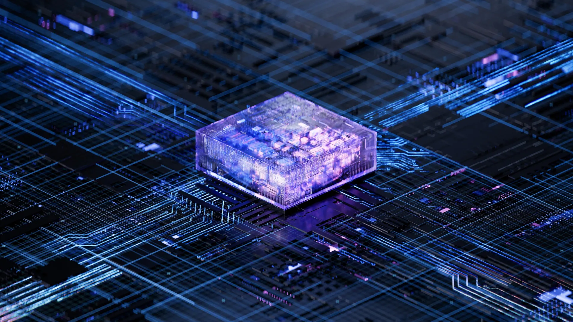
Researchers have developed a manufacturing process that stacks silicon circuits vertically, addressing a fundamental challenge that has prevented mass production of three-dimensional computer chips. The technique uses ultra-thin silicon membranes and low-temperature processing to create multiple functional layers within a single chip package, potentially extending Moore's Law as traditional horizontal miniaturization reaches physical limits.
The breakthrough tackles heat dissipation, a critical problem in stacked chip designs. When circuits are layered, thermal energy accumulates in inner layers, degrading performance and reliability. Low-temperature manufacturing prevents this buildup while maintaining the integrity of the silicon structures. Ultra-thin membranes allow electrical signals to pass efficiently between layers without significant performance loss.
This approach differs from previous 3D stacking attempts, which primarily bonded pre-manufactured chips together. The new method integrates multiple circuit layers during fabrication itself, enabling denser interconnections and better thermal management. Industry observers note this could boost transistor density without shrinking individual components further, a strategy becoming increasingly important as sub-5-nanometer manufacturing encounters quantum mechanical obstacles.
Moore's Law, the observation that transistor count doubles roughly every two years, has guided semiconductor progress for decades but is slowing dramatically. Companies like TSMC and Samsung are investing heavily in advanced packaging technologies, including chiplet designs and 3D integration, to maintain performance improvements. This silicon-stacking technique offers a complementary path forward.
The research demonstrates that vertical integration can deliver computing gains comparable to traditional miniaturization, with fewer technical obstacles. Manufacturers could produce faster processors and memory chips without expensive retooling for smaller fabrication nodes. However, challenges remain: heat removal from the innermost layers, interconnect reliability across multiple strata, and cost-effective manufacturing at scale all require further refinement.
The technique represents a pragmatic response to physics constraints rather than a revolutionary leap. Silicon stacking has long been theoretically